Welcome to Memorandum Deep Dives. In this series, we go beyond the headlines to examine the decisions shaping our digital future. 🗞️
This week, two of the world's most consequential chipmakers made announcements just four days apart, and on the surface, they looked like routine product updates. AMD confirmed that its next-generation server processor had entered production at the most advanced facility on Earth. Huawei, meanwhile, took the stage at a circuits conference in Shanghai to unveil what it described as a successor to one of the most important principles in modern computing.
Read separately, each announcement sounds like a milestone in a long-running technology race. Read together, they tell a more interesting story about where that race is actually heading, and who gets to participate in it.
The semiconductor industry has spent nearly six decades operating under a single, widely shared set of assumptions. What happened in May 2026 suggests those assumptions may no longer hold equally for everyone, and the implications stretch well beyond the companies involved.
In partnership with

Blu Dot surpasses 2,000% ROAS with self-serve CTV ads
Home furniture brand Blu Dot blew up on CTV with help from Roku Ads Manager. Here’s how:
After a test campaign reached 211,000 households and achieved 1,010% ROAS, the brand went all in to promote its annual sales event. It removed age and income constraints to expand reach and shifted budget to custom audiences and retargeting, where intent was strongest.
The results speak for themselves. As Blu Dot increased their investment by 10x, ROAS jumped to 2,308% and more page-view conversions surpassed 50,000.
“For CTV campaigns, Roku has been a top performer,” said Claire Folkestad, Paid Media Strategist, Blu Dot. “Comping to our other platforms, we have seen really strong ROAS… and highly efficient CPMs, lower than any other CTV partner we've worked with.”
Using Roku Ads Manager, the campaign moved from a pilot to a permanent performance engine for the brand.
Inside the fracture, splitting the global chip industry
For nearly six decades, the semiconductor industry advanced according to a simple and remarkably reliable principle: smaller transistors produced faster, cheaper, and more efficient chips. Popularly known as Moore’s Law after Gordon Moore, that idea became the foundation of modern computing, shaping everything from product roadmaps to the global technology economy. But the model has been slowing under the combined pressure of physical limits, rising manufacturing complexity, and the enormous cost of pushing silicon further.
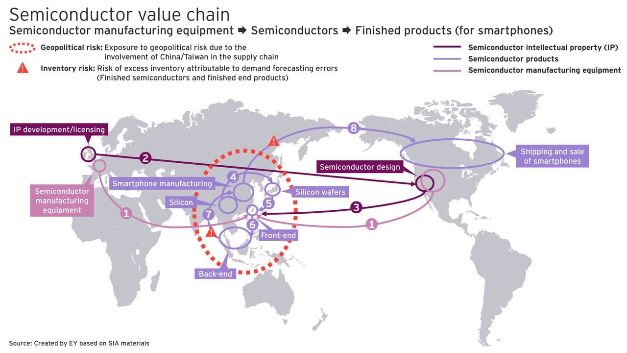
At the same time, the semiconductor industry itself is becoming less globally integrated. For decades, chipmaking depended on a deeply interconnected system in which American firms designed processors, Dutch companies built lithography machines, Taiwanese foundries manufactured chips, and Chinese factories assembled devices at scale. Increasingly, however, export controls, industrial policy, and geopolitical tensions are reshaping that arrangement into a more fragmented and politically constrained system.
Two announcements made four days apart in May 2026 captured that shift. AMD pushed further into the traditional frontier with next-generation 2nm chips built by TSMC, while Huawei unveiled a new architecture designed to work around the manufacturing limits imposed by U.S. export controls. Together, they suggest that the future of semiconductor progress may no longer follow a single shared roadmap, but increasingly divergent technological and geopolitical paths.
Huawei’s workaround: design what you can’t manufacture
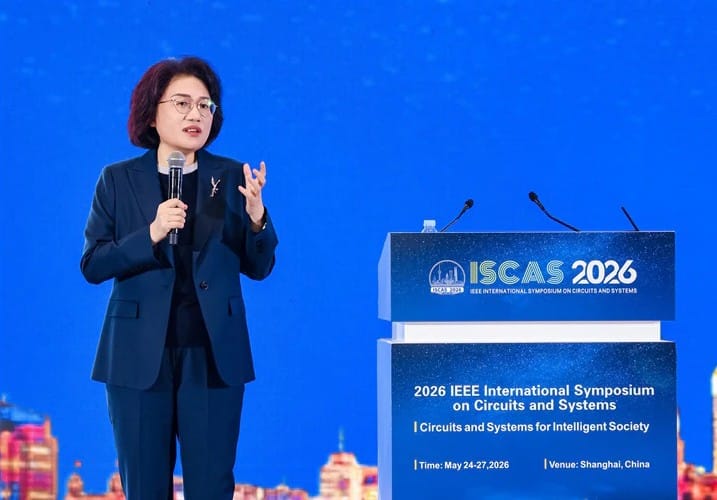
On May 25, at an IEEE circuits conference in Shanghai, Huawei semiconductor chief He Tingbo presented what the company calls the Tau (τ) Scaling Law, a proposed successor to Moore’s Law that changes the focus of chip design. Instead of trying to make transistors endlessly smaller, the idea centers on reducing the time it takes for signals to move across a chip.
The reasoning behind that shift lies in a growing problem inside modern processors themselves. As chips become denser and more complex, performance is increasingly constrained not only by transistor size but by the tiny amounts of resistance and capacitance carried by the microscopic wires connecting them, a form of electrical friction that slows communication across the chip. Huawei says its new architecture, called LogicFolding, is designed to address that bottleneck by stacking circuit layers vertically, shortening the distance signals need to travel rather than continuing the industry’s increasingly difficult pursuit of smaller transistors.
The trade-off of this approach is that vertically stacked architectures introduce new engineering challenges. As more circuitry is packed into tighter physical space, heat becomes significantly harder to dissipate, particularly in AI accelerators designed to sustain massive parallel workloads for extended periods.
AMD’s bet: own the frontier while it still exists
Four days before Huawei unveiled its new approach, AMD announced that its next-generation server processor, codenamed Venice, had entered production at TSMC’s 2-nanometer (2nm) facility in Taiwan, making it the first high-performance computing chip to reach that milestone.
A 2nm chip is not literally two nanometers in any single physical dimension. Instead, the label refers to a new generation of manufacturing technology that improves transistor density and energy efficiency over the chips that came before it. In practical terms, more computing power can be packed into the same amount of space while using less energy.
Outperform the competition.
Tools & resources, ranging from playbooks, databases, courses, and more.
Deep dives on famous visionary leaders.
Interviews with entrepreneurs and playbook breakdowns.
*This is sponsored content
Two answers to the same question
Even though the announcements emerged from very different technological and geopolitical environments, they are worth examining together because they represent two fundamentally different responses to the same underlying reality: the old rules that once governed semiconductor progress no longer apply equally to everyone.
For Huawei, the shift comes in response to the physical limitations of packing more transistors within limited space as well as political constraints.
Since 2019, U.S. export controls have steadily blocked Chinese companies from accessing EUV (extreme ultraviolet) lithography machines, the specialized equipment used by leading foundries to manufacture the world’s most advanced chips. Those machines are manufactured exclusively by the Dutch company ASML, making it the single most consequential chokepoint in the global semiconductor supply chain. Without access to EUV, Huawei’s manufacturing partner, SMIC, China’s largest domestic foundry, has had to rely on older and less precise machinery.
In practice, that means relying heavily on a technique known as multi-patterning, in which older DUV lithography systems make multiple passes to approximate the precision of newer EUV machines. The method works, but it is slower, more expensive, and generally produces lower yields, making advanced chips significantly harder to manufacture economically at scale.
The Tau Scaling Law is Huawei’s formal response to that gap. Rather than competing directly on TSMC’s terms, Huawei is attempting to redefine the terms by optimizing how quickly signals move through a chip rather than focusing exclusively on shrinking transistor size. Huawei says it has already built 381 chips using related principles over the past six years across smartphones and AI computing systems.
Yet many of the company’s claims remain difficult to verify independently. Unlike AMD’s 2nm milestone, which depends on TSMC’s commercially deployed manufacturing infrastructure, Huawei’s LogicFolding architecture has not yet undergone broad third-party benchmarking under large-scale AI workloads, which means it may have performed well in controlled demonstrations but has yet to prove itself in real-world conditions where heat, manufacturing yield, and power consumption become limiting factors.
AMD, by contrast, is pursuing the traditional frontier as aggressively as possible. The company reported $5.8B in data center revenue for the first quarter of 2026, up 57% year over year, while its EPYC server processors captured a record 46.2% share of server CPU spending during the period, according to Mercury Research data cited in AMD’s investor release. Venice is AMD’s attempt to extend that lead into the next generation of hardware.
What’s actually driving each bet
Beyond market and technological conditions, the strategies adopted by the two companies also reflect the geopolitical constraints increasingly influencing global tech.
Since Huawei cannot buy the manufacturing equipment, the Tau Scaling Law is, in part, an attempt to argue that the industry’s traditional benchmarks, process node, foundry access, and transistor size, are no longer the only meaningful measures of progress. If Huawei can achieve comparable performance through architectural design rather than cutting-edge lithography, then export controls become less decisive.
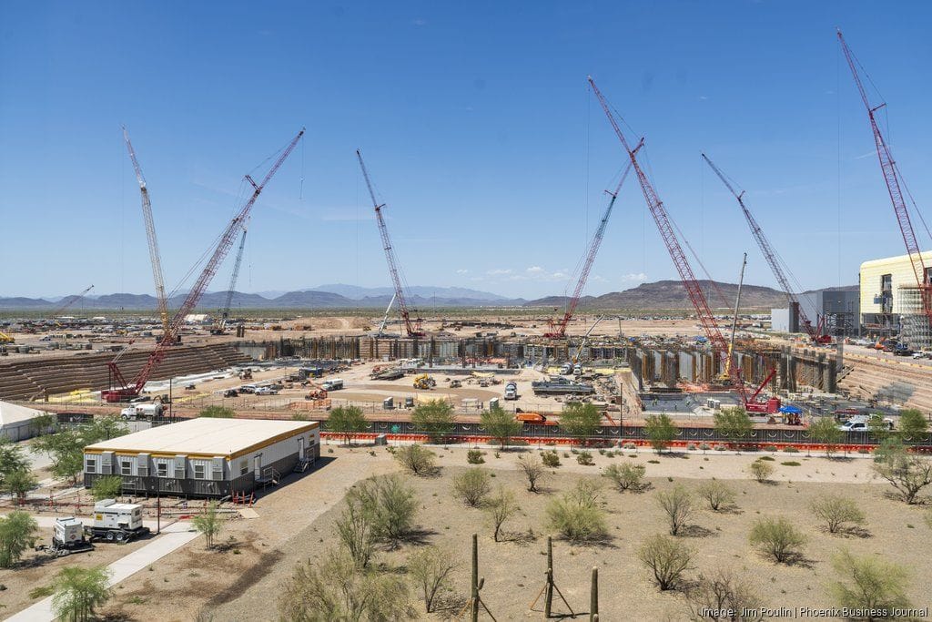
AMD’s strategy depends on a different kind of access: proximity to the only company currently capable of manufacturing chips at the absolute frontier. Venice entered production in Taiwan, with plans to eventually expand to TSMC’s Arizona facility, which was built in part with up to $6.6B in U.S. government funding through the CHIPS and Science Act. That plant currently handles 4nm production and is estimated to satisfy only a small fraction of U.S. chip demand, while 2nm production is not expected there until at least 2028.
What to watch next
For the broader industry, the good news is that neither company’s claims will remain untested for long. Huawei says the first Kirin smartphones with LogicFolding will launch in the fall of 2026, and analysts will likely examine them closely. The key question, then, will be whether the performance gains match the company’s claims and hold up when applied to AI processors that carry far heavier workloads than smartphones. Meanwhile, China’s older DUV lithography ecosystem continues to improve, with domestic foundries extending the capabilities of existing equipment through techniques like multi-patterning and the development of local scanner technology.
For AMD, the near-term test is whether Venice can sustain the company’s rapid growth in data centers. AMD has already tied part of that future to large-scale AI demand through infrastructure agreements with companies like Meta and supply arrangements with OpenAI, both of which ultimately depend on AMD’s ability to manufacture and deliver chips at scale.
However, neither announcement resolves the larger question of whether two parallel semiconductor ecosystems can evolve independently and still meet the demands placed on them.
Huawei’s framework may address chip design, but it does not solve the challenge of manufacturing those chips at the scale required for a national AI buildout using older equipment already operating under strain.
At the same time, AMD’s Venice pushes performance further at the frontier. Still, that frontier remains concentrated in Taiwan, precisely the dependency U.S. industrial policy is now trying to reduce, even as domestic alternatives remain years behind schedule.
For most of the past half-century, the semiconductor industry’s defining characteristic was interdependence. No single country could build a modern chip on its own, and that mutual reliance was, in its way, a stabilizing force. What Huawei and AMD are each building, in their separate directions, is a bet that interdependence is no longer a safe assumption. Whether either bet proves correct matters less, in the long run, than the fact that both felt compelled to make it.
P.S. Want to collaborate?
Share today’s news with someone who would dig it. It really helps us to grow.
Let’s partner up. Looking for some ad inventory? Cool, we’ve got some.
Deeper integrations. If it’s some longer-form storytelling you are after, reply to this email, and we can get the ball rolling.
What did you think of today's memo? |
|









.svg)
.svg)